
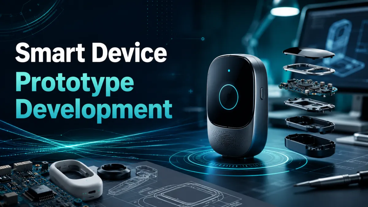
Essential Tips for Smart Device Prototype Development
Smart device prototypes combine electronic hardware, mechanical design, and connectivity in a single physical product. This makes them significantly more complex to develop than either pure electronics or pure mechanical products. Sensors, PCBs, batteries, antennas, and connectors all have to integrate into an enclosure that also has to meet industrial design, ergonomic, and manufacturing requirements. For inventors, entrepreneurs, and small business owners developing smart devices, understanding a few essential prototyping principles is what separates products that survive real use from products that reveal integration problems after tooling investment.
Quick Answer
Essential tips for smart device prototype development include: address hardware architecture (sensors, connectivity, processing, power) before locking down enclosure geometry; design the PCB and enclosure together rather than sequentially, since each constrains the other; plan for thermal management early, particularly for battery-powered or continuously-powered devices; consider RF and antenna behavior during enclosure design, since materials and geometry affect wireless performance; design for manufacturing assembly of electronic components, not just the enclosure; and plan for the regulatory testing the product will need before launch. These tips reduce the integration surprises that most first-time smart device inventors encounter. Full-service product development firms coordinate industrial design, mechanical engineering, PCB layout, and enclosure work as an integrated Phase 2 discipline for the hardware side of smart devices.
Key Facts
- Smart devices integrate electronic hardware, mechanical design, and connectivity in a single physical product
- Hardware architecture decisions (sensors, connectivity, processing, power) should shape enclosure design, not fit into it after the fact
- PCB layout and enclosure design constrain each other and should be developed in parallel
- Thermal management, antenna placement, and battery integration are common integration challenges
- Regulatory certification (FCC, CE, and similar) is performed by qualified testing labs; Phase 2 design work supports the certification the product will need
Key Takeaways
- Smart device prototyping requires coordinating multiple engineering disciplines simultaneously rather than sequentially
- The most common smart device prototype failures come from integration problems between electronics and mechanical design
- Thermal, RF, and battery considerations affect both PCB layout and enclosure design and have to be planned together
- Designing for the manufacturing assembly process for electronics is as important as designing for the enclosure production process
- Regulatory testing considerations should shape design decisions during Phase 2, not be discovered at Phase 3
- Structured Phase 2 work that integrates industrial design, mechanical engineering, PCB layout, and DFM review produces smart device prototypes that survive integration
Table of Contents
- What Makes Smart Device Prototyping Different
- Tip 1: Address Hardware Architecture Before Locking Down Enclosure
- Tip 2: Design PCB and Enclosure Together, Not Sequentially
- Tip 3: Plan for Thermal Management Early
- Tip 4: Consider RF and Antenna Behavior in Enclosure Design
- Tip 5: Design for Manufacturing Assembly of Electronics
- Tip 6: Design Decisions That Support Regulatory Testing
- How the Four-Phase Process Applies to Smart Devices
- How Rabbit Product Design Develops Smart Device Prototypes
What Makes Smart Device Prototyping Different
A smart device is more than the sum of its electronics and its enclosure. Sensors have to be positioned so they can sense what they’re meant to sense. Antennas have to be placed where they can transmit and receive. Batteries have to fit, be safely retained, and manage the heat they produce. PCB traces have to route around mechanical features. Buttons and controls have to interface with both the PCB and the user. Every one of these considerations depends on both the electronic design and the mechanical design working together.
This produces prototyping demands that pure-mechanical or pure-electronic products don’t face. A mechanical product prototype can validate mechanical performance in isolation. An electronic circuit can be validated on a bench before enclosure. A smart device needs the electronics and the mechanical design validated together — because integration issues only appear when both are present.
The result is that smart device prototyping is more coordination-intensive than either component discipline alone. Success depends on parallel work across multiple engineering disciplines, not sequential handoffs. This is where first-time smart device inventors most commonly encounter difficulty.
Tip 1: Address Hardware Architecture Before Locking Down Enclosure
The first essential tip is to define the electronic hardware architecture before finalizing enclosure geometry. Hardware architecture includes the sensors the device needs, the connectivity approach (wired, Bluetooth, Wi-Fi, cellular, or combinations), the processing and memory approach, the power source, and the user interface hardware (buttons, indicators, displays where applicable).
Why Architecture Comes First
Each architecture decision shapes what the physical product has to be. A device with a large sensor array needs a physical form factor that accommodates it. A cellular-connected device needs an antenna that works with the enclosure. A device running from a rechargeable battery needs charging hardware and battery mounting. Locking down enclosure geometry before architecture is settled produces enclosures that don’t fit the electronics they need to contain.
Common Architecture Pitfalls
Products often begin with an industrial design vision and try to fit the electronics into it. This can work for products with modest electronic requirements, but for anything with significant sensor, connectivity, or power requirements, the electronics have to shape the enclosure rather than the reverse. Architecture-first design produces devices that actually work; enclosure-first design often produces devices that look right but perform poorly.
Tip 2: Design PCB and Enclosure Together, Not Sequentially
The second essential tip is to develop the PCB layout and the enclosure design in parallel, treating them as one integrated design problem rather than two separate ones.
Why Parallel Design Matters
PCB layout determines where components sit — which determines where the enclosure has to accommodate them. Enclosure design determines mounting features, connector locations, and internal geometry — which determines where the PCB has to route around. Sequential design (PCB done first, enclosure designed around it, or vice versa) locks in decisions on one side that constrain the other. Parallel design lets both sides adjust to each other during Phase 2 iteration.
Common Integration Issues
When PCB and enclosure are designed separately, common issues include connectors that don’t align with enclosure openings, components that interfere with enclosure mounting features, PCB traces that route through areas the enclosure needs for mechanical strength, and mounting screws that conflict with PCB placement. Parallel design catches these issues in CAD before physical prototypes reveal them.
Tip 3: Plan for Thermal Management Early
The third essential tip is to plan for the heat the device will produce before enclosure design is complete. Any electronic device that draws meaningful power produces heat; enclosed devices can trap that heat if the design doesn’t account for it.
Sources of Heat in Smart Devices
Heat in smart devices comes from processors under load, wireless transmitters during operation, power regulation circuitry, batteries during charging or discharging, and any high-current components. Devices that spend most of their time in low-power modes may have modest thermal loads; devices that transmit continuously, run high-performance processing, or handle significant power may need active thermal management.
Thermal Design Considerations
Thermal design considerations include enclosure material thermal conductivity, venting or convection paths where applicable, heat-spreading features within the enclosure, thermal separation between heat-sensitive and heat-generating components, and battery thermal isolation for safety. Products where thermal design is addressed during Phase 2 avoid the field failures that thermal problems produce.
Tip 4: Consider RF and Antenna Behavior in Enclosure Design
The fourth essential tip is to account for wireless behavior when designing the enclosure. Materials, geometry, and internal components all affect how well wireless signals transmit and receive.
Materials and RF Performance
Metal enclosures can shield antennas, preventing signals from reaching or leaving the device. Plastic enclosures are generally more RF-transparent but material additives and coatings can still affect performance. Products with wireless requirements need enclosure material choices that support the wireless performance the product needs.
Antenna Placement
Antennas need to be positioned where they can radiate effectively — away from ground planes, metal components, and structural features that could block or detune them. Antenna placement is a joint decision between the PCB design and the enclosure design. Products that treat antenna placement as an afterthought often show poor wireless performance in field conditions.
Testing RF Performance
RF performance testing during Phase 2 validates that the physical implementation supports the wireless behavior the product needs. Products that skip early RF validation often discover wireless problems late in development when correcting them requires enclosure redesign.
Tip 5: Design for Manufacturing Assembly of Electronics
The fifth essential tip is to design for how the electronics will actually be assembled during production, not just how the enclosure will be produced.
PCB Assembly Considerations
PCB assembly in production has specific requirements: component placement for automated pick-and-place, appropriate solder pad geometries, panelization considerations, and test point access for in-circuit or functional testing. PCBs designed without production assembly considerations often work as hand-built prototypes but produce yield problems in mass production.
Enclosure Assembly Considerations
The assembly sequence for getting electronics into the enclosure matters. Which parts go in what order, how connectors mate during assembly, where fasteners are accessible, and whether the enclosure can be assembled without special tooling all affect production cost and quality. Products where assembly sequence isn’t validated on physical prototypes often reveal problems in production.
Testing and Programming Access
Many smart devices need functional testing and initial programming during production. Design features that support production testing — test points, connector access, LED indicators — make the production process more manageable. Products where testing access is added late often require enclosure modifications to accommodate it.
Tip 6: Design Decisions That Support Regulatory Testing
The sixth essential tip is to make design decisions during Phase 2 that support the regulatory testing the finished product will need. Regulatory certification itself is performed by qualified testing laboratories; the design decisions that make certification achievable are Phase 2 product development work.
Common Regulatory Requirements
Smart devices sold in the United States typically need FCC certification for wireless devices; devices sold in Europe typically need CE marking. Battery-powered devices may need battery safety certification. Devices with specific use claims (medical, industrial, safety) may have additional certification requirements. The specific certifications needed depend on the product’s functions and target markets.
Design for Certification
Design decisions that support certification include appropriate component selection (using components with existing certifications where possible), proper grounding and shielding for EMC performance, appropriate labeling space for regulatory markings, and design features that allow the testing lab to actually perform its tests. Products where certification requirements are understood during Phase 2 typically achieve certification more smoothly than products where certification is a Phase 3 discovery.
How the Four-Phase Process Applies to Smart Devices
The four-phase product development process organizes smart device work across a structured sequence that respects the coordination the discipline requires.
Phase 1 (Research & Ideation)
Phase 1 establishes target users, use conditions, functional requirements, unit economics, and regulatory awareness for target markets. For smart devices, Phase 1 also includes hardware architecture definition — the sensors, connectivity, processing, and power approach that will shape Phase 2 work.
Phase 2 (Design & Prototype)
Phase 2 executes industrial design, mechanical engineering, PCB layout, and component selection as parallel disciplines. Thermal, RF, and assembly considerations shape both electronics and mechanical decisions. Prototyping progresses through CNC machined enclosures with prototype PCBs, then soft tooling and injection molding samples for pre-production hardware validation.
Phase 3 (Sourcing & Manufacturing)
Phase 3 qualifies contract manufacturers with appropriate electronics assembly capability, first-article inspection of both enclosures and PCBs, and pilot production to validate the manufacturing process. Regulatory testing coordinated with qualified labs typically happens during Phase 3.
Phase 4 (Branding & Marketing)
Phase 4 launches the product through appropriate channels for smart devices — direct-to-consumer, retail, or specialty channels depending on the product category. Packaging often needs to communicate connectivity, battery life, and other smart device features clearly.
How Rabbit Product Design Develops Smart Device Prototypes
Smart device development requires coordinating industrial design, mechanical engineering, PCB layout, component selection, thermal management, RF considerations, and design-for-assembly across the hardware side of the product — a multi-discipline challenge that first-time inventors typically don’t have the experience to manage across separate vendors. Rabbit Product Design handles this integration under one roof. With 9 years in business, over 2,000 products developed, and senior engineers averaging 27 years of experience, the firm brings the coordination discipline that smart device prototypes require.
Smart devices fit in the electronic products and IoT vertical, one of the firm’s five verticals — consumer products, soft goods (bags, cases, wearables, sports gear, pet products), hardware (brackets, hinges, latches, mounting systems, mechanical assemblies, fixtures, storage hardware), electronic products and IoT, and inventor projects. Smart devices often also involve consumer product design (aesthetic and ergonomic considerations) and hardware components (structural mounting, mechanical assemblies). The scope covered is the hardware side: industrial design, mechanical engineering, PCB layout, component selection, enclosure design, and DFM review across these categories.
The Phase 2 discipline Rabbit Product Design brings to smart device prototypes includes hardware architecture definition informing enclosure design; parallel PCB layout and enclosure development; thermal design coordinated across electronics and mechanical; RF and antenna considerations built into enclosure design; design for manufacturing assembly of electronics; and design decisions that support the regulatory testing the product will need. Regulatory certification itself is coordinated with qualified testing laboratories.
For inventors developing smart devices, having engineers who coordinate the hardware disciplines together typically produces better integration than sourcing each discipline separately and hoping the outputs come together. Senior engineers with electronic product experience know which integration issues appear most often and how to structure Phase 2 to catch them early.
Smart Device Prototyping Services Across Phases
- Phase 1: research on target users, use conditions, functional requirements, unit economics, regulatory awareness, hardware architecture definition
- Phase 2: integrated industrial design, mechanical engineering, PCB layout, component selection, thermal and RF design; prototyping through CNC machining, soft tooling, and injection molding samples
- Phase 3: supplier qualification for electronics assembly capability, first-article inspection, pilot production, coordination with regulatory testing labs
- Phase 4: packaging communicating smart device features clearly, marketing suited to smart device channels and audiences
To begin a product development engagement for a smart device, contact Rabbit Product Design.
Conclusion
Essential smart device prototyping tips — addressing hardware architecture before enclosure, designing PCB and enclosure together, planning thermal management early, considering RF behavior in enclosure design, designing for manufacturing assembly of electronics, and making design decisions that support regulatory testing — each address a category of integration issue that produces smart device prototype failures when handled poorly. For inventors, entrepreneurs, and small business owners developing smart devices, structured Phase 2 work that coordinates industrial design, mechanical engineering, PCB layout, and DFM review as integrated disciplines produces prototypes that survive integration and support the regulatory testing the product will need.
FAQ
What makes smart device prototyping different from typical product prototyping?
Smart devices integrate electronic hardware, mechanical design, and connectivity in one physical product. Sensors, PCBs, batteries, antennas, and connectors all have to work together within an enclosure that also meets industrial design, ergonomic, and manufacturing requirements. This requires multiple engineering disciplines working in parallel rather than sequentially, and the most common failure modes come from integration issues between electronics and mechanical design that only appear when both are present.
Should I design the PCB or the enclosure first?
Neither should be finalized before the other — they should be developed in parallel because each constrains the other. PCB layout determines where components sit, which determines what the enclosure has to accommodate. Enclosure design determines mounting features and internal geometry, which determines where the PCB has to route around. Sequential design produces integration problems; parallel design lets both sides adjust during Phase 2 iteration.
How do I plan for thermal management in a smart device?
Identify the sources of heat in the device (processors under load, wireless transmitters, power circuitry, batteries), estimate the thermal load in expected use, and design the enclosure to dissipate that heat appropriately. Considerations include material thermal conductivity, venting or convection paths where applicable, heat-spreading features, and thermal separation between heat-sensitive and heat-generating components. Thermal design should be part of Phase 2, not discovered at Phase 3.
What regulatory testing does a smart device need?
Depends on the product’s functions and target markets. Wireless devices sold in the United States typically need FCC certification; devices sold in Europe typically need CE marking. Battery-powered devices may need battery safety certification. Devices with specific use claims may have additional certification requirements. Regulatory certification itself is performed by qualified testing laboratories; the design decisions that make certification achievable are Phase 2 product development work.
Who helps inventors develop smart device prototypes end-to-end?
A full-service product development firm that handles industrial design, mechanical engineering, PCB layout, component selection, thermal and RF design, enclosure design, DFM review, and manufacturing coordination under one engagement on the hardware side. Firms integrating these disciplines cover smart devices, which fit within a dedicated electronic products and IoT product vertical.